A laser engraver can make PCBs by engraving circuit patterns, drilling holes, and cutting PCB outlines.
When choosing a laser engraver for PCB prototyping, laser type and precision matter. Real-world results range from around 100 μm-class PCB traces to features as fine as about 20 μm.
This guide compares fiber and UV lasers for PCB work, explains what affects achievable feature size, and shows what you can realistically expect when choosing a machine for PCB prototyping.
What Can a Laser Do to a PCB?
| PCB application | What the laser does | Typical workflow | Main challenge |
| Direct copper ablation | Removes unwanted copper directly from a copper-clad laminate | Laser → finished copper pattern | Removing the copper without excessive damage to the FR4 substrate |
| Resist-layer ablation | Removes selected areas of resist while leaving the copper underneath | Laser → chemical etching | Adds a chemical etching step and requires control of under-etching |
| Solder-mask removal | Removes selected areas of solder mask to expose copper pads | Laser → exposed copper pads | Stopping at the copper layer without unnecessarily damaging the pad |
| Isolation-slot machining | Removes a narrow strip of copper between conductive areas | Laser → electrical isolation | Maintaining a clean, continuous insulating gap |
| Drilling | Creates holes in the PCB, including through holes or blind microvias | Laser → drilled hole or via | Controlling hole diameter, taper, depth, and heat-affected material |
| Board cutting | Cuts the PCB substrate along its outline or separates sections of a board | Laser → finished PCB profile | Controlling kerf, edge quality, heat damage, and debris |
Why Is Fine PCB Laser Processing Challenging?
1.Spot Size Is Not Feature Size
Laser processing also generates heat, so the affected area can extend beyond the beam size. A 0.01 mm spot does not automatically produce a 0.01 mm trace. Meanwhile, thermal effects, beam profile, focus, pulse parameters, scanning strategy, material absorption, and copper thickness can all affect the final feature.
2.Copper Removal Must Be Controlled
Too little energy can leave copper residue and prevent electrical isolation. Too much energy can damage the FR-4 underneath. Selective copper removal therefore requires balancing copper ablation with substrate damage.
3.Substrate Damage Can Affect Insulation
Excessive heating can carbonize the epoxy in FR-4. Carbonized material may become conductive, creating leakage paths or even shorts.
4.Processing Method Matters
With laser-assisted chemical etching, underetching can change the final dimensions. Direct copper ablation avoids wet etching but requires tighter control of heat and substrate damage.
How Fine Can a Fiber Laser Process PCB?
The following experiments show how copper thickness, substrate, laser system, optics, and processing method affect how fine a fiber laser can process a PCB.
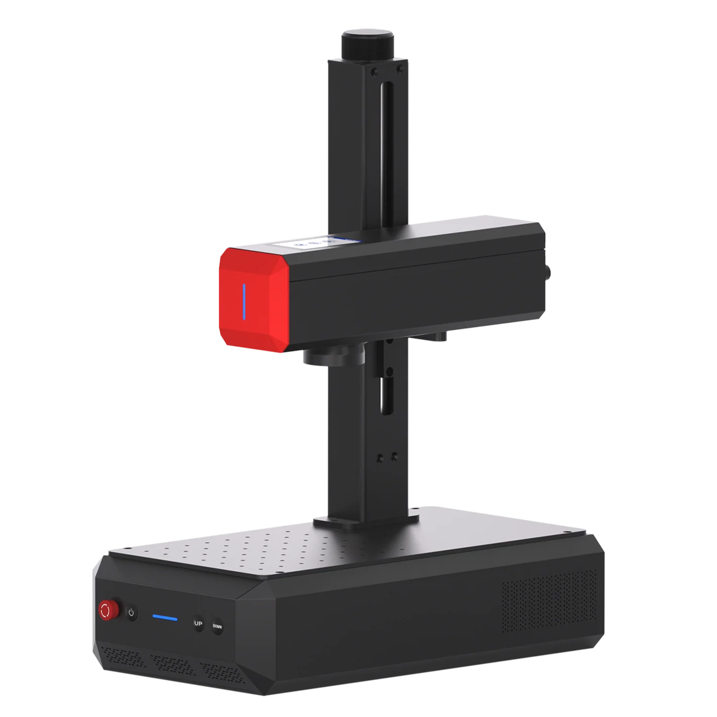
Case 1: Double-Sided FR-4 PCB with a ComMarker B4 20W
Material: Copper-clad PCB laminate, 110mm lens
Process:
- Check and clean the copper-clad board with alcohol and sponge
- Laser the top copper layer: Speed 160 mm/s, power 95%, 37 kHz, 1 pass.
- Clean the copper traces with brush and check with multimeter
- Apply UV-curable solder mask and cure under UV light.
- Laser remove the solder mask from component pads without intentionally removing the copper underneath: speed 100 mm/s, power 25%, 37 kHz, 0.04 mm hatch spacing.
- Partially drill the holes
First drilled partway from the top then flip and continued from the bottom: speed 150 mm/s, power 75%, 2 passes, followed by 150 mm/s at 85% power for five passes. - Process the bottom copper layer
After repositioning the flipped board, the bottom copper pattern was processed using: speed 150 mm/s, power 100%, and 37 kHz. - Remove the bottom solder mask and complete the holes.
- Cut the finished PCB outline: speed 30 mm/s, power 100%, 37 kHz, and 3 passes.
Result: Arduino Uno-style PCB with 0.15 mm clearance, solder mask, exposed pads, drilled holes, and aligned top and bottom copper layers.
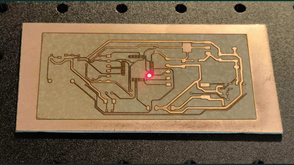
Case 2: FR-4 PCB laser engraving with MOPA Fiber Laser
Material: Copper-clad FR-4 PCB laminate
Why MOPA: MOPA fiber lasers provide greater control over pulse frequency and pulse duration. For PCB processing, this additional control can help tune how much energy is delivered to the copper and how the laser interacts with the underlying substrate, helping produce cleaner and more repeatable results.
Marking parameters (60W MOPA): Speed 800 mm/s, Power 80%, Frequency 38 kHz, Pulse width 20 ns, line distance 0.02
Result: An FR-4 PCB with 0.05 mm designed traces.
How Fine Can a UV Laser Process PCB?
A 355 nm UV laser is particularly useful when PCB processing moves toward fine-pitch traces, narrow isolation gaps, and small features. Its shorter wavelength allows a smaller focused spot than many infrared systems, while UV laser processing can be tuned to limit unwanted thermal effects.
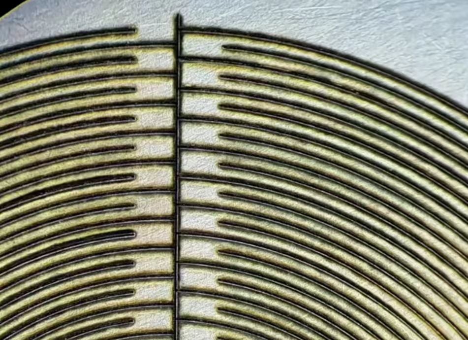
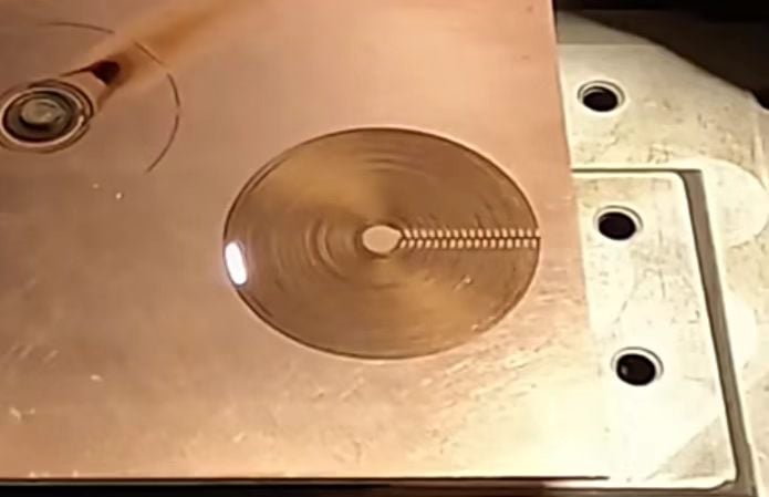
Case: 355 nm UV Laser Direct Patterning on FR-4 PCB
Material: FR-4 PCB with 18 μm or 35 μm copper layers
Laser system: 12W UV laser
Process: The laser directly ablated the copper layer to create grooves and conductive tracks.
Settings: Speed 2000mm/s, freq 40, pulse 23, 70mm lens.
Result:
18 μm copper: minimum groove width about 11 μm, minimum track width about 20 μm
35 μm copper: minimum groove width about 13 μm, minimum track width about 40 μm
 |
 |
*The above case results are experimental reference values. As PCB engraving results depends on the copper thickness, PCB substrate, optics, focus, and processing strategy.
Notes for Laser Engraving PCB
Laser processing FR-4 and other PCB materials can generate fumes and fine particles. Use appropriate laser safety measures, ventilation, and fume extraction.
Check the PCB Condition
Before starting, confirm the PCB substrate, copper thickness, surface finish, and existing coatings.
Also check that the board is clean, flat, and securely positioned. A warped or moving PCB can change the working distance and make fine features less consistent. For fine PCB processing, use a vacuum bed or other flat holding platform to keep the PCB securely flat during processing.
Use Proper Fume Extraction
Laser processing PCB materials can generate fumes, particles, and laser-generated airborne contaminants. Use appropriate local exhaust or fume extraction to control contaminants rather than relying only on general room ventilation.
Which ComMarker Laser Should You Choose for PCB Prototyping?
Fiber Laser: Practical Beginner Choice for PCB Prototyping
A basic fiber laser is a practical choice for PCB prototyping because it can remove copper efficiently while also handling common metal marking, engraving, and cutting tasks.
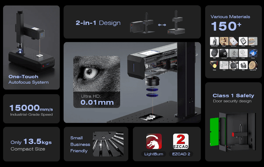
The ComMarker B6 Fiber Laser features:
- 15,000 mm/s Engraving Speed: enables efficient copper removal for PCB prototyping.
- 8K HD Accuracy with 0.01mm spotsize: helps produce clean and consistent PCB patterns.
- Up to 200 × 200 mm Engraving Area — provides enough working space for larger PCB prototypes.
The main limitation is process control compared with MOPA fiber lasers. A conventional fiber laser offers a narrower range of pulse parameters, so fine-tuning the interaction between the laser, copper, and FR-4 can be more limited.
MOPA Fiber Laser: More Control for Repeatable PCB Processing
A MOPA fiber laser is useful when PCB processing requires more control over how laser energy interacts with the copper and substrate. Compared with a conventional fixed-pulse fiber laser, MOPA technology provides a much wider range of pulse width and frequency adjustment, making it easier to tune the ablation process for different copper thicknesses and PCB materials.
The ComMarker B6 JPT MOPA Fiber Laser features:
- JPT MOPA Laser Source: provides adjustable pulse parameters for more precise control of copper ablation.
- 15,000 mm/s Engraving Speed: supports efficient material removal while testing different PCB processing parameters.
- Up to 300 × 300 mm Engraving Area with Optional Lens — accommodates larger PCB prototypes and different workpiece sizes.
This wider pulse-control range gives users more flexibility to develop and reproduce a PCB processing recipe, rather than relying on a single fixed laser configuration.
UV Laser: For the Finest PCB Features
A 355 nm UV laser is better suited when the priority shifts from general copper removal to fine features and delicate processing. The shorter wavelength allows a very small focused spot, while UV processing can reduce unwanted thermal effects compared with longer-wavelength infrared processing under suitable conditions.
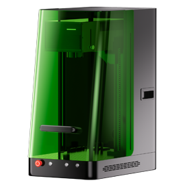
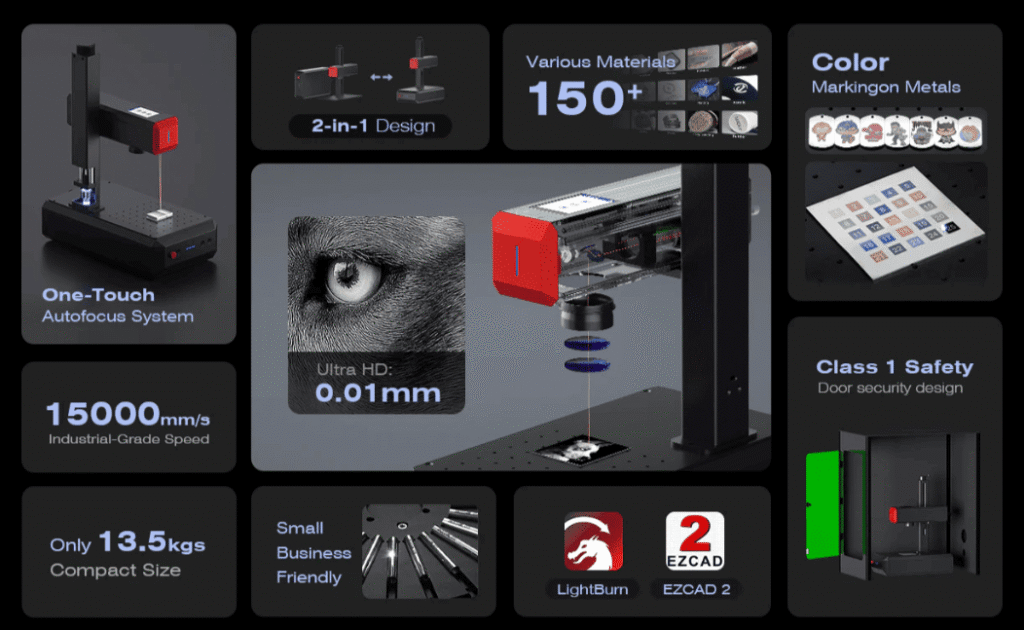
The ComMarker Omni X UV Laser features:
- 16K HD Accuracy with 0.0019 mm Laser Spot Dimension: supports fine PCB patterns and narrow isolation gaps.
- ZeroBurn™ Engraving Technology: helps minimize unwanted thermal effects when processing delicate PCB features.
The main limitation is material-removal efficiency. A UV laser is much slower than a higher-power fiber laser when removing large amounts of copper or cutting thick materials. Its strength is precision rather than bulk material removal.

Final Thoughts
Laser PCB processing is not simply about matching copper thickness, trace width, clearance, laser type, focus, and processing parameters. These factors work together to determine the smallest feature you can produce reliably.
A 20W fiber laser is a practical starting point for general PCB prototyping and efficient copper removal. A MOPA fiber laser provides greater control over pulse parameters, making it more suitable when you need to fine-tune and reproduce a specific PCB processing result. A 355 nm UV laser is better suited to very fine features and delicate processing, with slower bulk material removal as the trade-off.
Before choosing a laser, define your required trace width, clearance, copper thickness, and PCB substrate, then choose a machine based on your requirements.
Explore ComMarker’s fiber, MOPA fiber, and UV laser engravers to find a PCB processing setup that matches your application.